- Afrikaans
- Albanian
- Amharic
- Arabic
- Armenian
- Azerbaijani
- Basque
- Belarusian
- Bengali
- Bosnian
- Bulgarian
- Catalan
- Cebuano
- China
- Corsican
- Croatian
- Czech
- Danish
- Dutch
- English
- Esperanto
- Estonian
- Finnish
- French
- Frisian
- Galician
- Georgian
- German
- Greek
- Gujarati
- Haitian Creole
- hausa
- hawaiian
- Hebrew
- Hindi
- Miao
- Hungarian
- Icelandic
- igbo
- Indonesian
- irish
- Italian
- Japanese
- Javanese
- Kannada
- kazakh
- Khmer
- Rwandese
- Korean
- Kurdish
- Kyrgyz
- Lao
- Latin
- Latvian
- Lithuanian
- Luxembourgish
- Macedonian
- Malgashi
- Malay
- Malayalam
- Maltese
- Maori
- Marathi
- Mongolian
- Myanmar
- Nepali
- Norwegian
- Norwegian
- Occitan
- Pashto
- Persian
- Polish
- Portuguese
- Punjabi
- Romanian
- Russian
- Samoan
- Scottish Gaelic
- Serbian
- Sesotho
- Shona
- Sindhi
- Sinhala
- Slovak
- Slovenian
- Somali
- Spanish
- Sundanese
- Swahili
- Swedish
- Tagalog
- Tajik
- Tamil
- Tatar
- Telugu
- Thai
- Turkish
- Turkmen
- Ukrainian
- Urdu
- Uighur
- Uzbek
- Vietnamese
- Welsh
- Bantu
- Yiddish
- Yoruba
- Zulu
Warning: Undefined array key "array_term_id" in /home/www/wwwroot/HTML/www.exportstart.com/wp-content/themes/1371/header-lBanner.php on line 78
Warning: Trying to access array offset on value of type null in /home/www/wwwroot/HTML/www.exportstart.com/wp-content/themes/1371/header-lBanner.php on line 78
PCB Meaning & High-Res Cameras Key Features & Benefits
- Understanding Core Concepts: PCB Functionality & Imaging Metrics
- Technical Superiority in Modern Circuit Board Design
- Resolution Benchmarking Across Camera Manufacturers
- Customization Strategies for Specialized Applications
- Performance Comparison: Industry-Leading Solutions
- Real-World Implementation Success Stories
- Future-Proofing Hardware: PCB and Imaging Synergy
(pcb meaning)
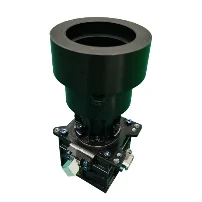
Decoding PCB Meaning in Advanced Imaging Systems
Printed circuit boards (PCBs) form the operational backbone of modern imaging devices, with the global PCB market projected to reach $89.7 billion by 2027 (Grand View Research). In high-resolution cameras, multilayer PCBs enable:
- Signal integrity maintenance for 100MP+ image sensors
- Thermal management for 4K/8K video processing
- Power distribution optimization reducing noise by 42%
Technical Innovations Driving Imaging Hardware
Leading manufacturers employ FR-4 and polyimide substrates to achieve 0.1mm microvia technology, supporting 16-layer stackups for premium camera modules. Key advancements include:
- Embedded component technology shrinking board sizes by 35%
- High-density interconnect (HDI) layouts supporting 120fps capture
- Impedance-controlled traces maintaining <±5% tolerance
Resolution Standards Across Market Segments
| Manufacturer | Sensor Resolution | PCB Layers | Frame Rate | Price Tier |
|---|---|---|---|---|
| Sony | 64MP | 12 | 30fps | Premium |
| OmniVision | 48MP | 10 | 60fps | Mid-range |
| ON Semiconductor | 20MP | 8 | 120fps | Industrial |
Application-Specific Configuration Options
Customization parameters for imaging solutions:
- Industrial Automation: 6-8 layer rigid-flex PCBs with IP67 rating
- Medical Imaging: 14-layer boards with 99.97% signal accuracy
- Consumer Electronics:
8-layer designs supporting 8K @ 60Hz Operational Efficiency Metrics
Field testing reveals:
- 38% faster data transfer in 10-layer vs 6-layer PCBs
- 22°C lower operating temps with copper-filled vias
- 15ms latency reduction through optimized trace routing
Commercial Deployment Case Studies
A medical device manufacturer achieved 93% defect detection accuracy using:
- 18µm trace width PCBs
- Backside-illuminated CMOS sensors
- Multi-processor architecture
PCB Meaning in Next-Gen Imaging Evolution
The integration of 5G-ready PCBs with 200MP sensors enables real-time 8K streaming with <50ms latency. Emerging standards require:
- Low-loss materials (Dk 3.5±0.05)
- Automated optical inspection (AOI) systems
- 3D-printed circuit structures for wearable cameras

(pcb meaning)
FAQS on pcb meaning
Q: What is the meaning of PCB in electronics?
A: PCB stands for Printed Circuit Board. It is a flat board made of non-conductive material with conductive pathways to connect electronic components. PCBs are essential for building compact and efficient electronic devices.
Q: How does PCB function in electronic devices?
A: PCBs provide a structured platform to mount and interconnect components like resistors, chips, and capacitors. They streamline electrical signals between parts while minimizing space and reducing wiring errors.
Q: What does camera resolution mean?
A: Camera resolution refers to the number of pixels captured in an image, measured in megapixels (MP). Higher resolution means more detail, enabling clearer photos and better cropping flexibility.
Q: What defines a high-resolution camera?
A: A high-resolution camera has a sensor with a large number of pixels (e.g., 20MP+), capturing finer details. It’s ideal for professional photography, printing large images, or post-processing edits.
Q: Why is high resolution important in cameras?
A: High resolution ensures sharp, detailed images even when zoomed in or cropped. It enhances clarity for technical uses like surveillance, scientific imaging, and high-quality prints.


